Inversion Semiconductor
Scaling chips down to their physical limits 15x faster
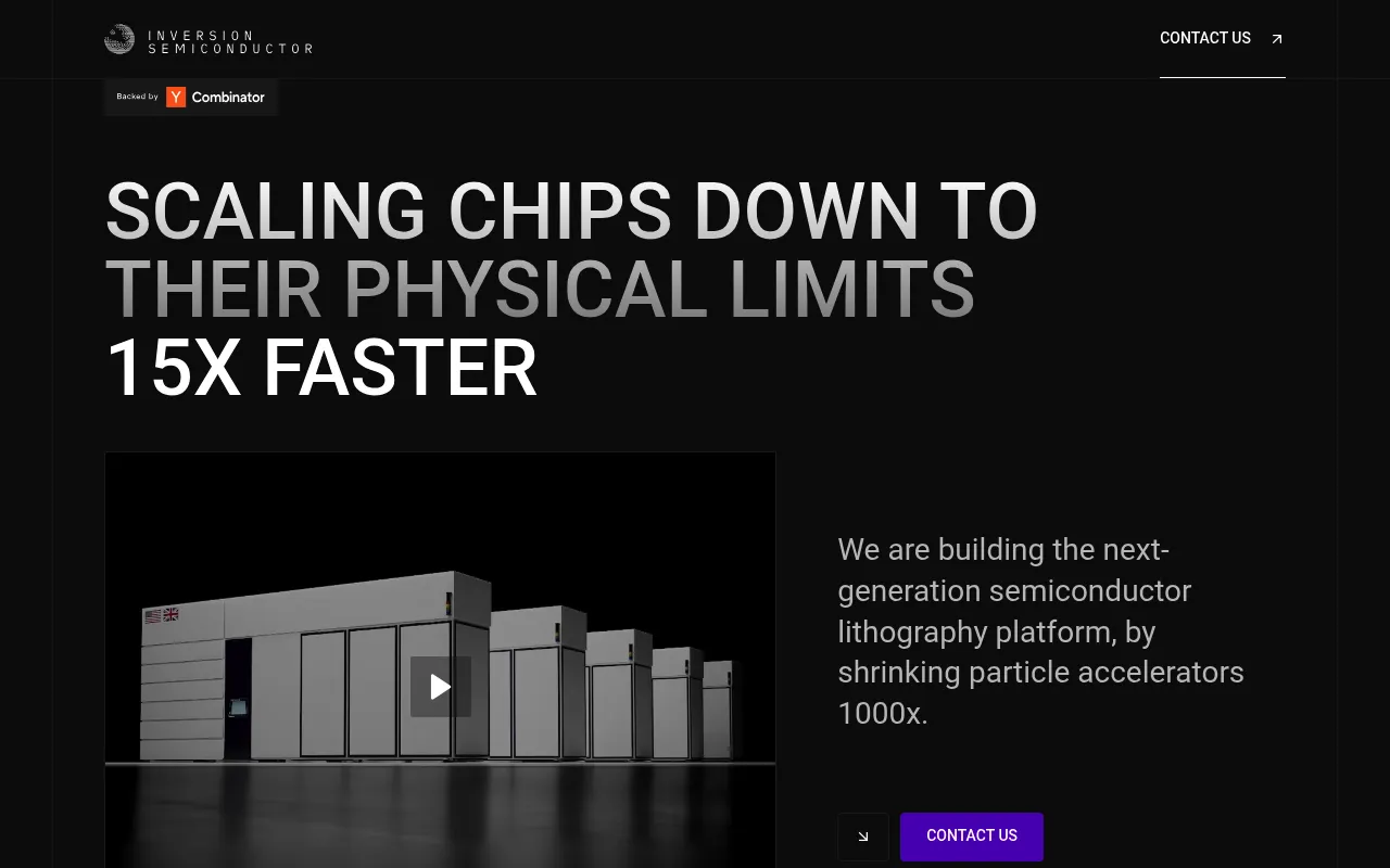
Inversion Semiconductor is building a next-generation semiconductor lithography platform by miniaturizing particle accelerators 1000x. Their compact accelerator serves as a high-power, tunable EUV light source aimed at dramatically improving transistor density, throughput, and critical dimension uniformity. The technology targets chip fabrication at the physical scaling limits, with applications in quantum and reversible computing architectures.
The company shrinks a particle accelerator 1000x to create a compact, high-power, tunable EUV light source that enables denser transistors, higher scanner throughput, and improved critical dimension uniformity.
Semiconductor manufacturers and chip fabrication facilities
Background.
- Status
- waitlist
- Business model
- unknown
- Company
- Inversion Semiconductor Inc.
Founders
- Rohan Karthik
- Daniel Vega
Similar projects.
Editorial take on the space this project sits in — momentum signals, adjacent moves, our call on whether the wedge is real. Get pinged when we publish a new read or when the landscape shifts.
Have a take on this space?
Tell us what you’d build differently, where you think the incumbents miss, or what we’ve gotten wrong about this project. Comments + reactions are coming soon.